Tunable two-dimensional (2D) materials open up revolutionary new opportunities as testbeds for manipulation and control of the properties of quantum matter at the atomic scale, and as platforms for nanoscale components in electronics and quantum computing.
Proximity Induced Superconductivity in Monolayer MoS2
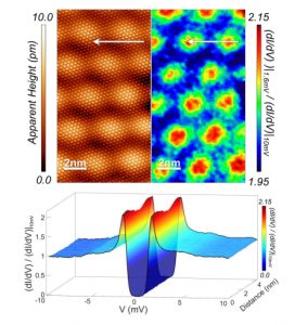
Atomic resolution STM image and corresponding conductance map of of the proximity induced gap in MoS2/Pb heterostructure.
The local atomic-scale geometry of the interface between Pb and MoS2 plays a key role in inducing superconductivity in an intrinsically semiconducting single-layer MoS2. Low temperature STM/STS topographic and spectroscopic images show that the atomic arrangement at the interface is responsible for the observed lattice-mismatch-related moiré patterns. Ab-initio electronic structure calculations and Green’s function-based methods unravel the presence of a two-step process that drives the formation of superconducting pairs in MoS2 and indicate a spatial modulation in superconducting pairing due to local variations in overlaps of atomic orbitals.
These results suggest that local modulation of induced superconducting pairing in MoS2 may be tuned geometrically, and in this way, our study introduces a new pathway for integrating proximity-induced monolayer superconductors into functional electronic devices. ACS Nano 14(3), 2718-2728 (2020)
Strain Relaxation Effects on the Local Electronic Properties of Monolayer MoS2
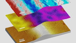
STM topographic, spectroscopic and strain maps of a rippled MoS2 single layer induced by strain.
The ability to control nanoscale electronic properties by introducing macroscopic strain is of critical importance for the implementation of 2D materials into flexible electronics and next generation strain engineering devices. The visualization of strain maps on the atomic scale and the correlation with the local effect on the quasiparticle density of states show changes in the band gap induced by strain and strain relaxation mechanisms taking place in monolayer MoS2. The strain is relaxed through the formation of one-dimensional ripples and two-dimensional wrinkles which alter the spatial electronic density of states. ACS Nano 13(7), 8284-8291 (2019)
Evolution of Metastable Defects in Monolayer MoS2
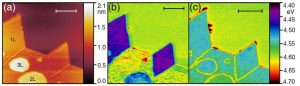
Topography map and Kelvin probe maps of changes in work function of MoS2 film after annealing.
An integrated approach, bringing together UHV Kelvin probe, high-resolution TEM and low temperature STM/STS shows that in MoS2 films metastable values of the work function are associated with the evolution of crystal defects formed during annealing or e-beam thermal activation. Sulfur vacancies formed after exposure to elevated temperatures are shown to diffuse, coalesce, and migrate to bring the system from a metastable to an equilibrium ground state. Scientific reports 8, 6724 (2018)
Defects in Monolayer MoS2
Intrinsic, atomic scale defects are the driving force behind many macroscopic electronic phenomena in two-dimensional (2D) materials and provide routes to manipulate and functionalize electronic properties to realize higher performance electronic devices. npj 2D Mater Appl 6, 13 (2022)
Spatial variation of the local density of states at defects sites in single layer MoS2 shows the presence of mid-gap states.